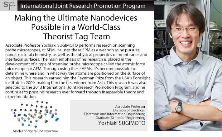
Making the Ultimate Nanodevices Possible in a World-Class Theorist Tag Team
Learning from World Class Resident Researchers
The atomic force microscope (AFM) can create images of individual atoms, while measuring and manipulating their physical properties. The AFM serves as the leading-edge of nanotechnology, a field with significant technological advancements both in Japan and around the world. There is a demand for the development of methods for investigating which element a particular atom is, not just its location. Associate Professor SUGIMOTO is continuing his cutting-edge research for this new technology. But at the same time, theoretical studies and computations are being sought after for things like how can the differences in types of atoms be identified, as well as what the differences in measured results are. “Experiments and theories are inseparable,” said Associate Professor SUGIMOTO.
There are few researchers on the theoretical side of this field, which makes the reality of the situation a global scramble. The group led by Pavel Jelínek at the Czech Academy of Sciences has an advantage on this theoretical side. Said Associate Professor Sugimoto, “I invited Professor Jelínek as a visiting professor to Osaka University, and this concentrated collaborative research has really brought vitality.” In addition, through seminars and discussions in English, OU students are developing their English ability, the ability to state their logic in English to foreign individuals, as well as their international-mindedness.
"Technology to Examine Time Resolution and Various Physical Quantities"
Through the refinement of semiconductive devices and the development of catalytic chemistry, measuring type, number, and position of atoms has become necessary. The one to answer the urgent request of this era was the scanning tunneling microscope, or STM, developed by Heinrich Rohrer (1986 Nobel laureate in physics) and his team, specifically Gerd Binnig.
When the tip of the probe is brought very close (1nm) to the surface of the sample, electric current begins to flow through the quantum effect.
Through this change in current, each individual atom on the sample surface is able to be identified. Further expansion of this lead to the atomic force microscope (AFM), which measures not electrical current, but the energy working between atoms to examine the sample surface. Using the AFM, even monoatoms of insulating specimens in which electricity does not flow, can be observed.
Associate Professor Sugimoto continues his research on the world’s leading edge. He is currently challenging not only the position of monoatoms, but also the discernment of elements and identifying atomic species. “We are already able to identify tin, lead, and silicon. Currently, the technology to discern representative elements such as oxygen and nitrogen has come into view,” said a bright-eyed Associate Professor Sugimoto. He added, “I want to establish the technology to measure not only spatial resolution, but also time temporal resolution and various physical quantities at the atomic level.”
Assembling Nanoclusters
AFMs are not only used for examining; it is also possible to move a singular atom using the tip of the probe. Associate Professor Sugimoto performed this operation under room temperature (25 degrees C or lower) conditions for the first time in the world. Combined with this, one can line up a singular atom of the necessary type at the desired position. This makes creating the literal ultimate in nanodevices possible. Expanding on this manipulation, an “atomic pen,” which plants one atom in the desired location, is being developed.
In July of 2014, he and his team developed the method for freely constructing nanoclusters consisting of multiple elements, and this was included in Nature Communications, vol.5, (2014) 10.1038. This is a method for provoking atom transfer which crosses over nanospace through chemical bonding force between the probe and monoatom. Monoatoms of elements such as gold, silver, and lead are counted one by one as they are inserted in a lattice-like silicon surface. For example, if one atom of gold and one atom of lead are packed together, this creates the world’s smallest “alloy,” one that completely reaches the limits of physics.
These results signify the creation of nanoclusters according to a preliminary design of the number and composition of atoms. This means that mankind is only one step away from the completion of the ultimate monoatomic nanotechnology that Feynman proposed. By using nanoclusters created through this manipulation, one can examine what kind of changes take place in their electronic and chemical characteristics depending on their size and composition. This holds a lot of promise if it is linked to the development of new materials and devices that will carve the way for future generations.
About Associate Professor Yoshiaki SUGIMOTO
A graduate of the Department of Physics, School of Science, Osaka University in 2001, Associate Professor Yoshiaki SUGIMOTO received his doctorate degree in engineering from the Division of Electrical, Electronic and Information Engineering at the Graduate School of Engineering in 2006. After serving as a specially appointed instructor at the Frontier Research Base for Global Young Researchers at the Frontier Research Center, Graduate School of Engineering, he began at his current position as Associate Professor in 2011. In 2012, he also began simultaneously working as a faculty member at the Institute for NanoScience Design. Associate Professor SUGIMOTO has also won various awards, such as the Minister of Education, Culture, Sports, Science and Technology Prize for Science and Technology (Research Category) in 2009, the 11th Japanese Society of Microscopy Prize in 2010 for his research on “Atom identification and manipulation at room temperature using non-contact atomic force microscopy,” and The Henrich Rohrer Medal (Rising Medal) in November, 2014.